

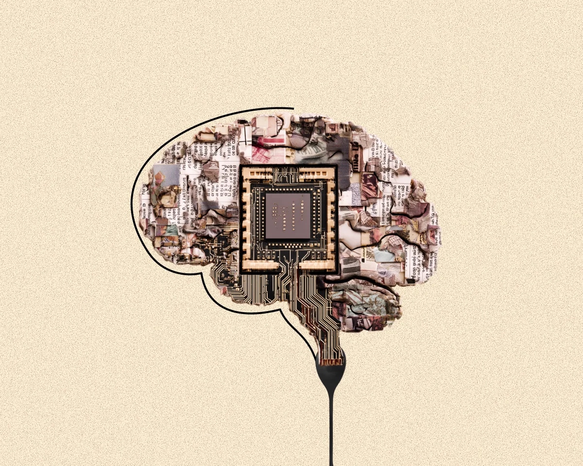
Set in silicon
How AI chips overcome the 'memory wall'
Consumer GPU have traditionally been built for video games and rendering. Yet they can also tackle other tasks that demand parallel computation.
A graphics processor can, for instance, run a PoW miner to mine cryptocurrencies, but competition from specialised rigs has pushed GPU farms into niches.
A similar story is playing out in AI. Graphics cards have become the mainstay for neural networks. As the industry has advanced, demand has risen for dedicated AI hardware. ForkLog examines the current state of this new lap in the artificial-intelligence race.
Optimising silicon for AI
There are several approaches to building hardware specialised for AI tasks.
Consumer GPUs are the starting point for specialisation. Their prowess at parallel matrix maths proved handy for deploying neural networks and, especially, deep learning, but there was ample room for improvement.
One of the chief problems of running AI on a GPU is the need constantly to shuttle large volumes of data between system memory and the GPU. These housekeeping chores can take more time and energy than the useful computation itself.
Another issue stems from GPUs’ generality. Their architecture caters to a wide range of jobs—from graphics rendering to general-purpose compute—leaving some hardware blocks redundant for targeted AI workloads.
Data formats pose a further constraint. Historically, graphics processors were tuned for FP32—32-bit floating-point numbers. Inference and training typically use lower-precision formats: 16-bit FP16 and BF16, or integer INT4 and INT8.
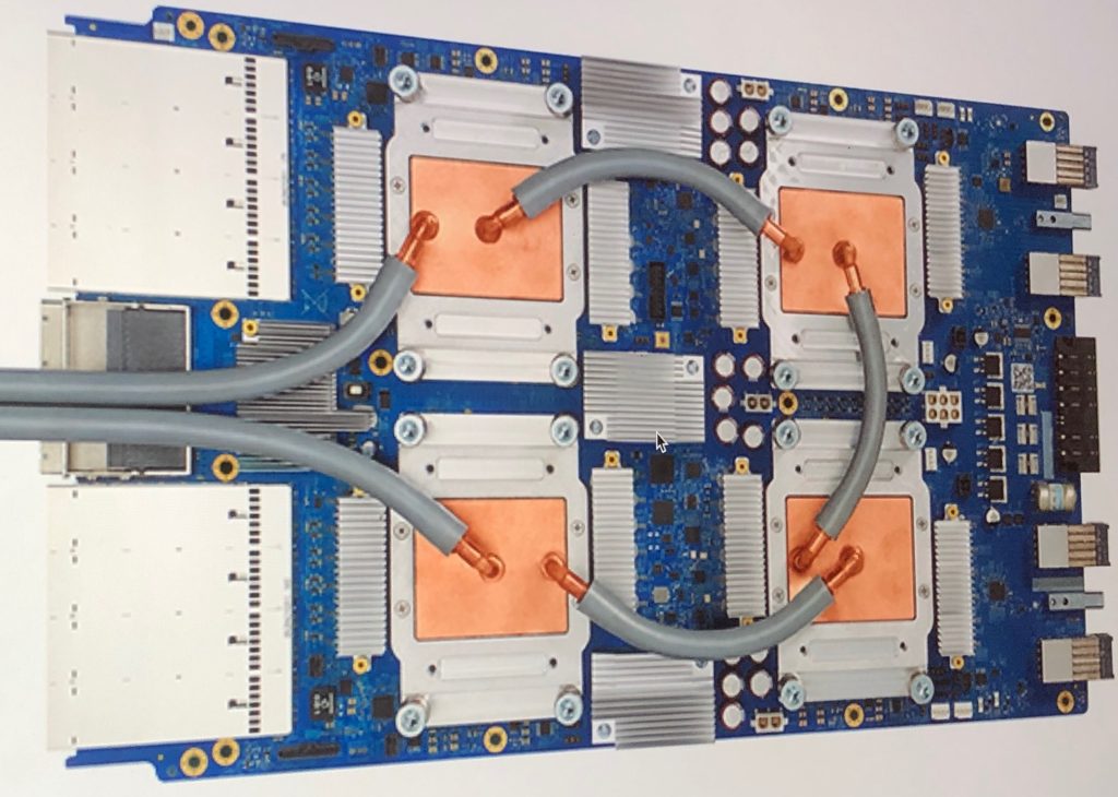
Nvidia H200 and B200
Some of the most popular products for inference and training—H200 chips and DGX B200 server systems—are, in essence, beefed-up GPUs for data centres.
The core AI-oriented feature of these accelerators is tensor cores, designed for ultra-fast matrix operations such as training models and batch inference.
To cut data-access latency, Nvidia equips its cards with vast amounts of high-bandwidth memory (HBM). The H200 integrates 141GB of HBM3e delivering 4.8TB/s; on the B200 the figures are higher still, depending on configuration.
Tensor Processing Unit
By 2015 Google had developed the Tensor Processing Unit (TPU), an ASIC built on systolic arrays for machine learning.
In conventional CPU and GPU architectures, each operation entails reading, processing and writing intermediate data to memory.
The TPU streams data through an array of blocks, each performing a mathematical operation and passing the result to the next. Memory is touched only at the beginning and end of the computation sequence.
This approach spends less time and energy on AI maths than a non-specialised GPU, though reliance on external memory remains a constraint.
Cerebras
American firm Cerebras has figured out how to use an entire silicon wafer as a single processor, instead of dicing it into smaller chips.
In 2019 the company introduced its first 300mm Wafer-Scale Engine. In 2024 it released the improved WSE-3, a 460mm die with 900,000 cores.
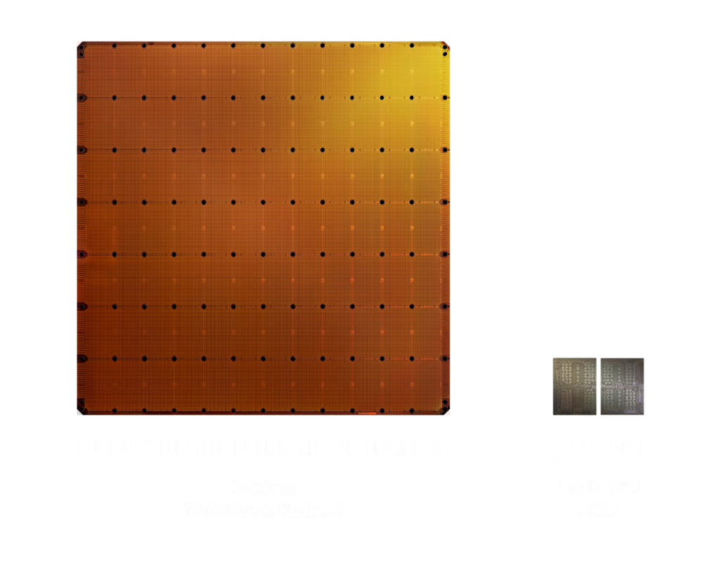
The Cerebras architecture distributes SRAM blocks right next to logic modules on the same wafer. Each core works with its own 48KB of local memory, avoiding contention with other cores.
According to the company, a single WSE-3 suffices for many inference workloads. For larger jobs, multiple chips can be clustered.
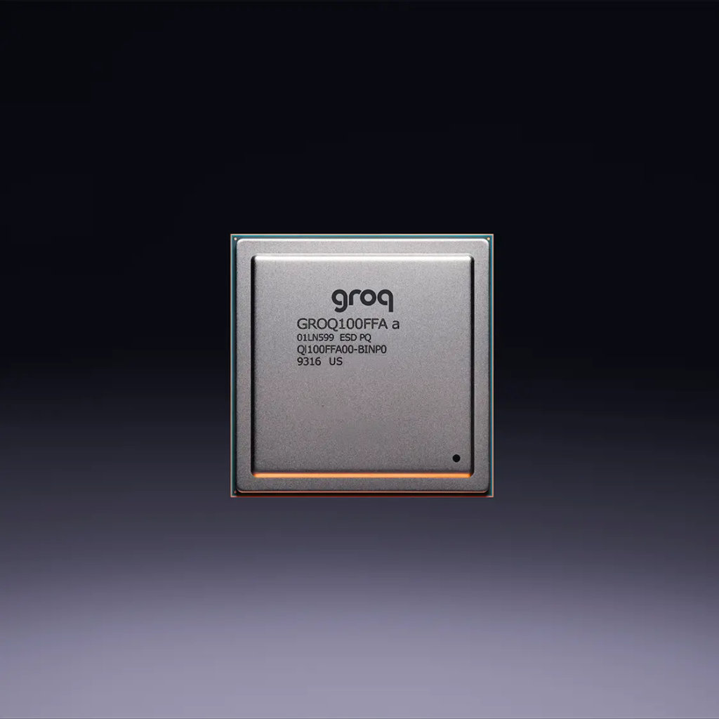
Groq LPU
Groq (not to be confused with Grok from xAI) offers its own inference ASIC built on a Language Processing Unit (LPU) architecture.
One key trait of Groq’s chips is their optimisation for sequential operations.
Inference generates tokens step by step: each step must finalise the previous one. Under such constraints, performance depends more on the speed of a single stream than on the number of streams.
Unlike familiar general-purpose processors—and some AI-specialised devices—Groq does not assemble machine instructions on the fly. Every operation is pre-planned in a sort of “schedule” and pinned to a specific moment in the processor’s work.
As with several other AI accelerators, the LPU combines logic and memory on one die to minimise data movement.
Taalas
All of the above assume a high degree of programmability: the model and its weights are loaded into rewritable memory. At any moment an operator can swap in a different model or tweak it.
With this approach, performance hinges on memory availability, speed and capacity.
Taalas goes further, choosing to hard-wire a specific model with fixed weights directly into the chip at the transistor level.
What is usually software becomes hardware, eliminating the need for a separate general-purpose data store—and the costs that come with it.
In its first product, the HC1 inference card, the company used the open Llama 3.1 8B model.
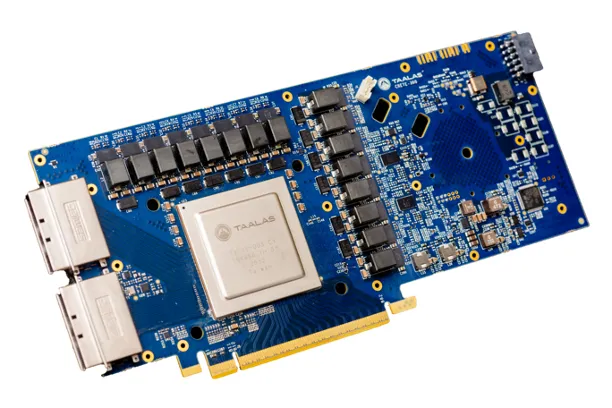
The card supports low-bit precision down to 3-bit and 6-bit parameters, speeding up processing. According to Taalas, the HC1 handles up to 17,000 tokens per second while remaining relatively inexpensive and power-thrifty.
The firm touts thousandfold performance gains over GPUs on a cost-and-power basis.
Such hard-wiring, however, has a fundamental drawback: the model cannot be updated without replacing the chip.
Even so, the HC1 supports LoRA, a method for fine-tuning LLM by adding extra weights. With the right LoRA configuration, a model can be turned into a specialist in a particular field.
Another difficulty is the design and manufacturing process for such “physical models”. ASIC development is costly and can take years—a serious constraint in a fast-moving AI market.
Taalas says it has a new method for generating processor architectures to address this. An automated system converts a model and weight set into a finished chip design within a week.
By the company’s own estimates, the production cycle—from receiving a new, previously unseen model to shipping chips that embody it in hardware—will take about two months.
The future of local inference
New specialised AI chips are first landing in vast data-centre installations, powering metered cloud services. The more radical options—even “physical models” realised directly in silicon—are no exception.
For consumers, the engineering leap will show up as cheaper services and faster response.
At the same time, simpler, cheaper and more energy-efficient chips lay the groundwork for widespread local inference.
Specialised AI chips are already in smartphones and laptops, security cameras and even doorbells. They enable local processing with low latency, autonomy and privacy.
Radical optimisation—even at the expense of flexibility in choosing and swapping models—greatly expands what such devices can do, allowing simple AI components to permeate cheap mass-market products.
If most users begin routing their queries to models that run on local devices, the load on data-centre capacity may ease, reducing the risk of overstrain. Perhaps then there will be no need to seek radical ways to expand compute—such as launching it into orbit.
Рассылки ForkLog: держите руку на пульсе биткоин-индустрии!